|
This research is carried out in the framework of Matheon supported by
Einstein Foundation Berlin.
|
Research goal and background
|
The goal of the iMatheon project D-OT8: Modeling, analysis, and optimization of optoelectronic semiconductor devices driven by experimental data is to optimize the design of a strained germanium microbridge with respect to the light emission.
In the funding period June 2016-December 2018 we will develop tools for the parameter identification and optimal design of experiment for optoelectronic applications. The project also involves the close collaboration with the Department for Materials Research at IHP (Leibniz-Institute for Innovative High Performance Microelectronics, Frankfurt Oder).
A cross-section through a typical material design of a strained microbridge is shown in Figure 1. The key idea is to increase the optical gain by applying a strong mechanical strain together with high doping. The dependence of gain on strain is captured by tight-binding calculations developed at IHP in collaboration with Pisa University [R2]. These results are included into van Roosbroeck-type models for semiconductors and equations for the optical field [R1] by an upscaling procedure [1].
Further details can also be found in publication [4] from the
WIAS Annual Research Report 2015.
|
|
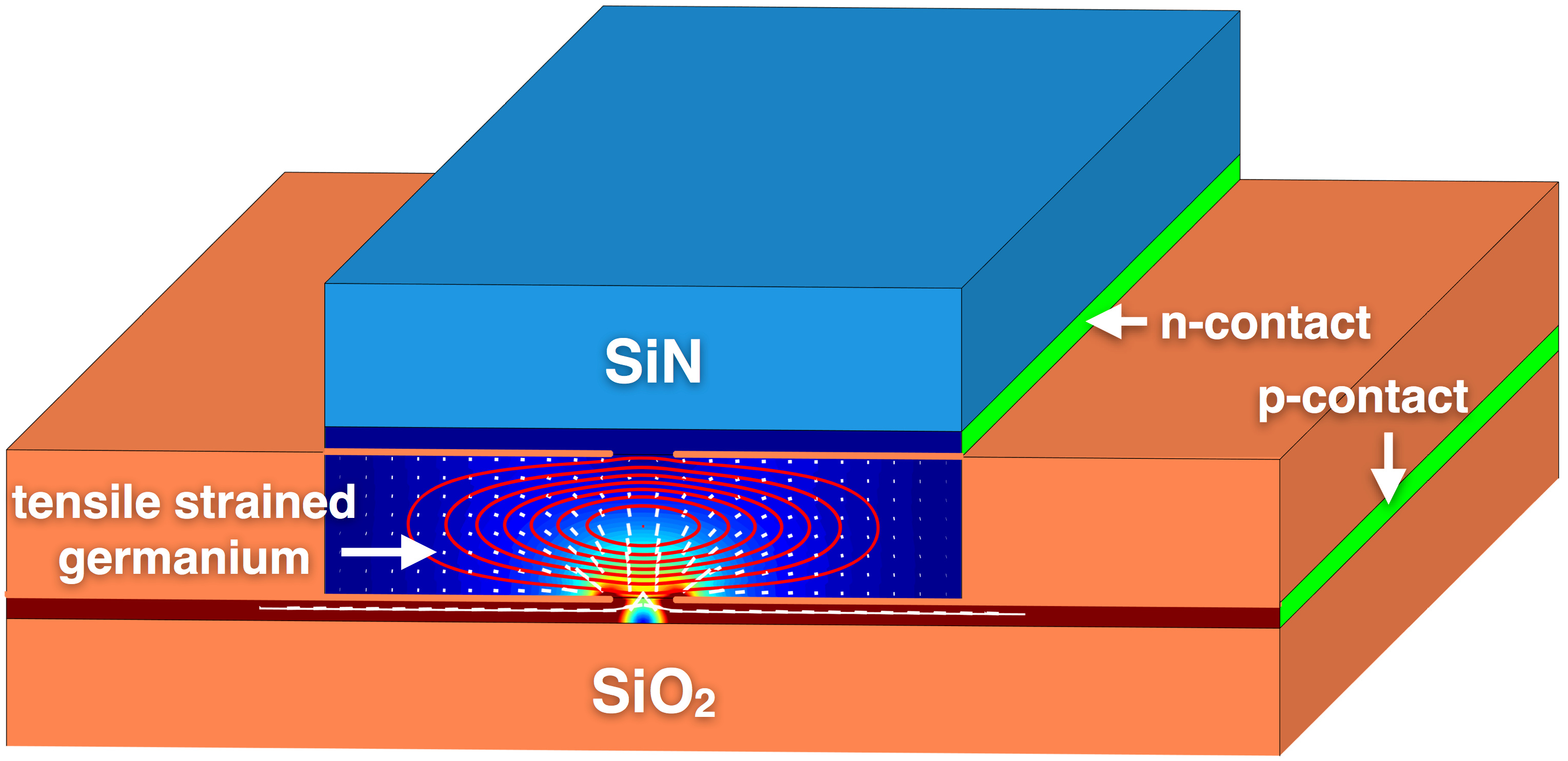
Figure 1: schematic cross section through a germanium microbridge, indicating optical mode and current densities
|
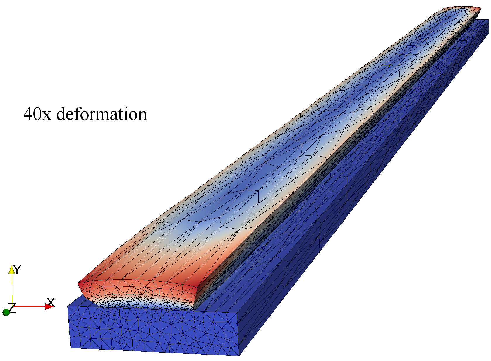
Figure 2: Deformation of the microbridge due to SiN stressor layer on top
|
|
Mathematical modelling of the strained heterostructure
The macroscopic PDE model for the mechanics, the carrier transport, the optics has the following components
- van Roosbroeck system for electricstatic ψ and quasi-Fermi potentials φ (1a),
- waveguide equation for optical mode in semiconductor Θ (1b),
- rate equation for the photon number S (1c),
- small strain linear elasticity for strain e(u) of an anisotropic material (1d),
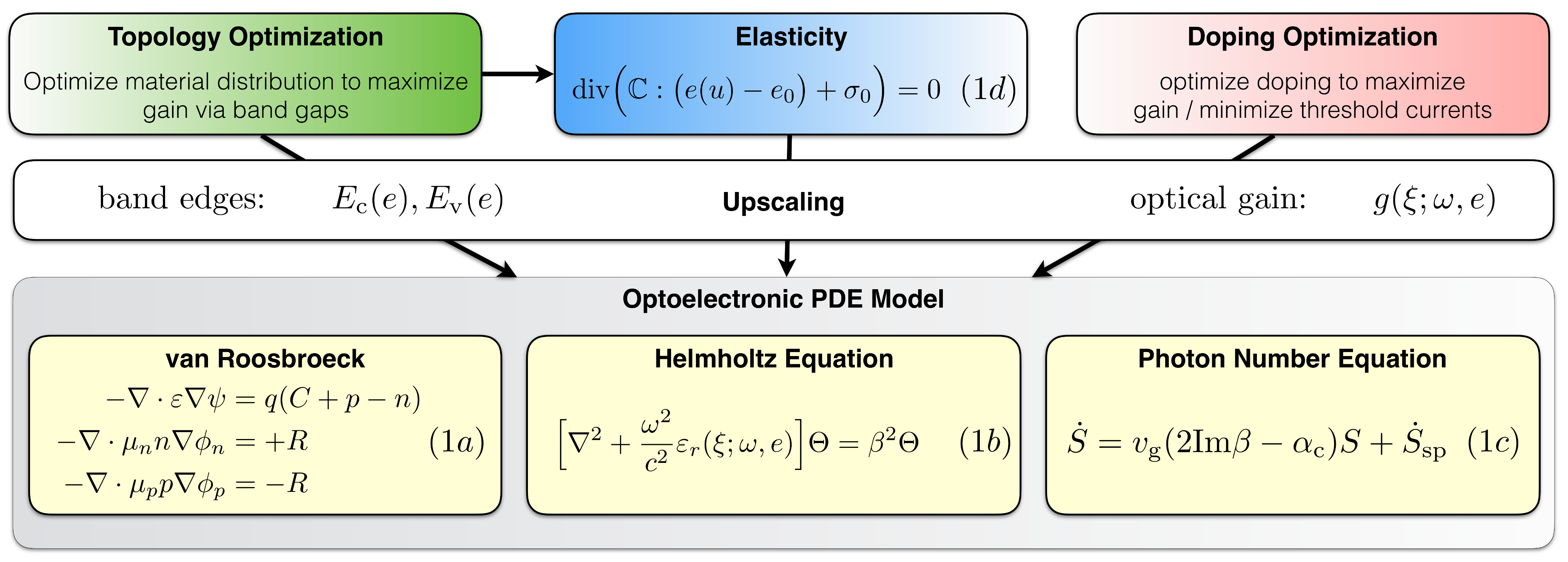
Linear elasticity (1d) can be solved independently. The strain e and doping C then influence the band-structure and optical gain g.
|
For details about equations (1a-1f) refer to [R1]. One important detail in the model is the dependence of the gain g on the strain, which can be found in recent works by our collaborators Virgilio et al. in [R2]. Joining both approaches by upscaling is a topic of our recent publication [1]. The biaxial strain used there matches with experiments and theory from [R3].
Mathematical optimization
Within the Matheon project OT1/8 we determine the optimal design of a Ge microstrip based on the optimization of optical properties (the photonic cavity and the optical mode), of mechanical strain, and of the doping profile. Due to the complexity of the underlying system, the shape optimization and the doping optimization are carried out separately.
|
Thus, the design/control variables of the microbridge are
- phase field variables ϕi for i=(Ge,SiO2,SiN,air) determining the material distribution,
- doping density C, determining the background concentration of carriers in the van Roosbroeck system,
based on which the device design will be optimized.
|
|
|
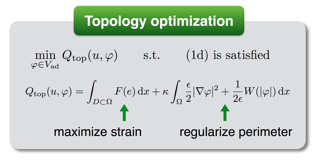
Topology optimization: The aim here is to determine an optimal configuration of the given materials within a domain Ω such that the band-gap is minimized by maximizing a suitable strain F within a given optical cavity D while adhering to a small strain setting. For the modeling of this, a phase-field approach is chosen, i.e., the fraction of each material within Ω is given by the corresponding component of the phase-field vector φ.
|
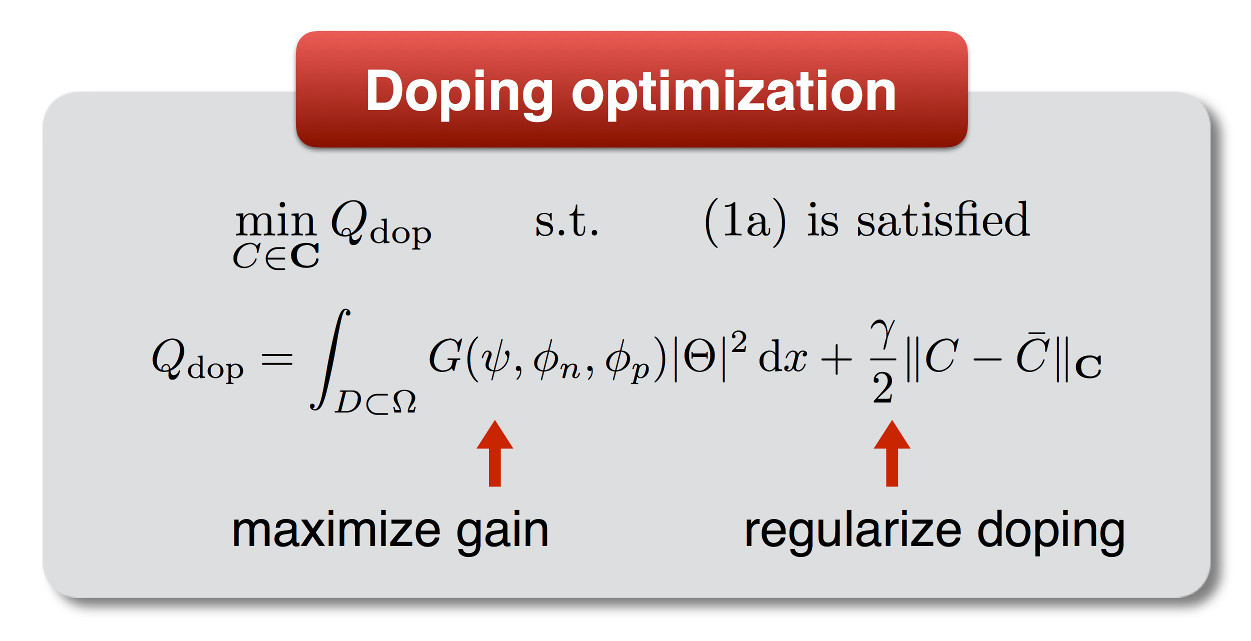
Doping optimization: The goal is to find an optimal doping profile C, for which the (negative) net-gain G=l-g containing gain g and losses l is minimal, so that we achieve the largest possible net-gain. We only need to achieve large gain in regions, where the optical mode Θ is localized, which is why only the overlap GΘ² needs to be maximized. However, one still needs to study the dependence on the regularization, i.e. on γ, C and the reference doping
C.
|
Doping optimization
The doping optimization attempts to improve optoelectronic features of an design, where cost functionals could be designed towards delivering high modal gain or low electrical currents (for instance at a fixed bias), the latter leading to doping configurations capable of creating doping pockets that guide the electrical current into the center of the optical mode, see Figure 4.
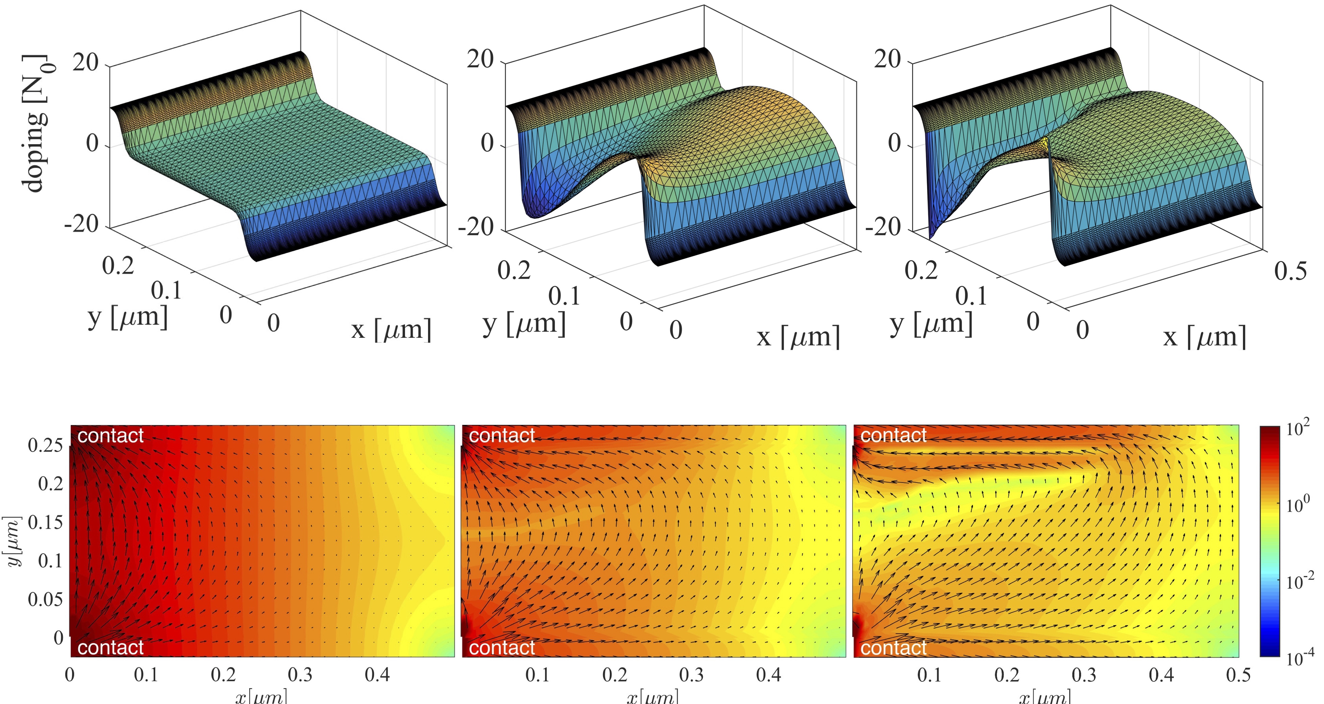
Figure 4: Different optimized dopings (left) reference (middle) gain oriented (right) current oriented goal.
|
Topology optimization
Here we highlight some exemplary results for the topology optimization of germanium microbridges.
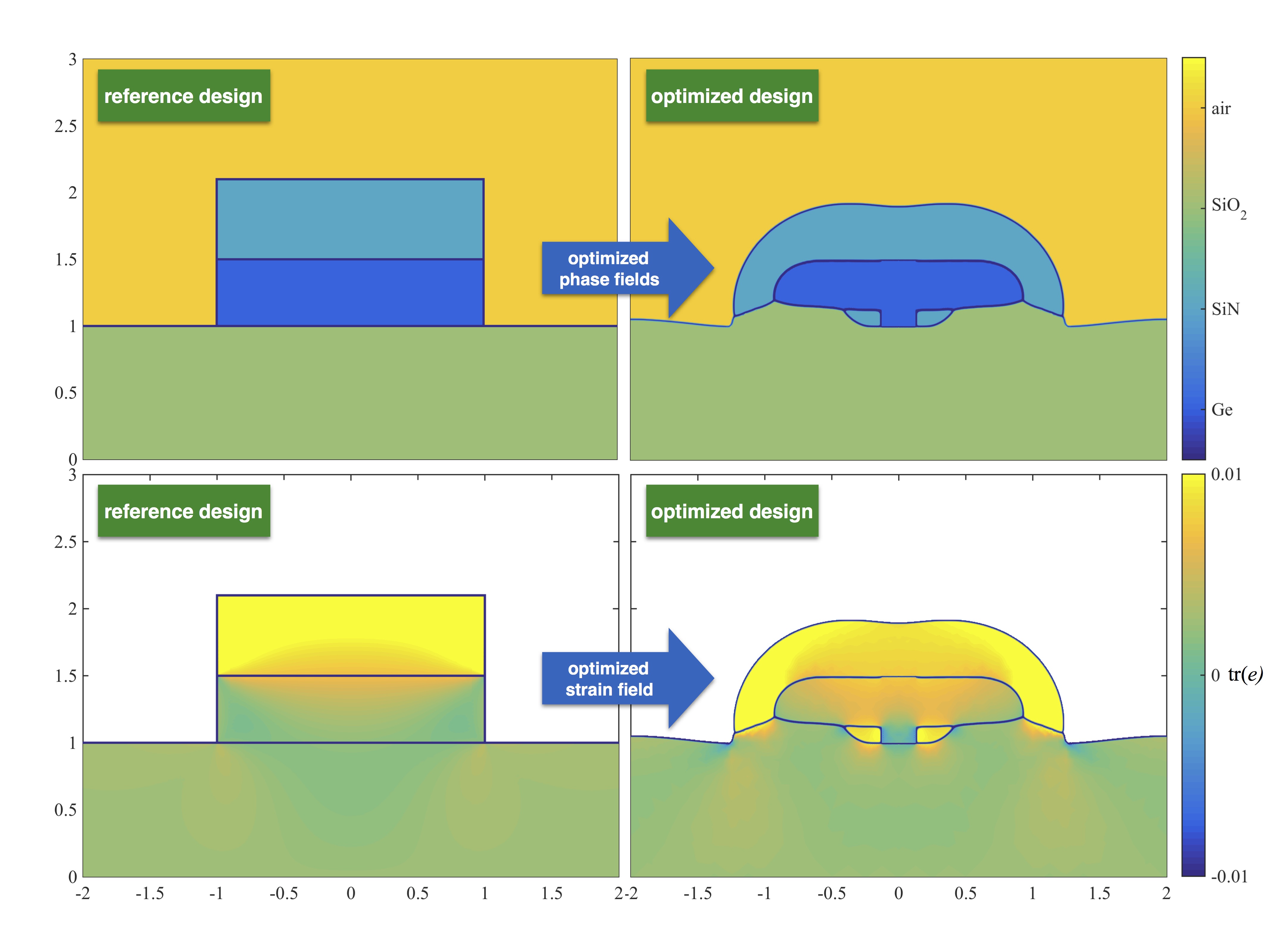
Figure 3: Different device topologies (left) reference microbridge (right) optimized microbridge cross section showing (top) phase fields and (bottom) strain fields.
|
The topology optimization produces improved device designs with large strain in the germanium cavity showin in Figure 3. The reference design with top SiN stressor (left panel) can, using a similar sized germanium cavity, be improved by an all-around-stressor design (right) obtained by the topology optimization. As desired, Figure 4 shows that the optimized design has significantly higher modal gain (upper panels) when comparin reference and optimized design. Furthermore, the inclusion of an aperature should deliver a much lower threshold current, as it has been observed in the past.
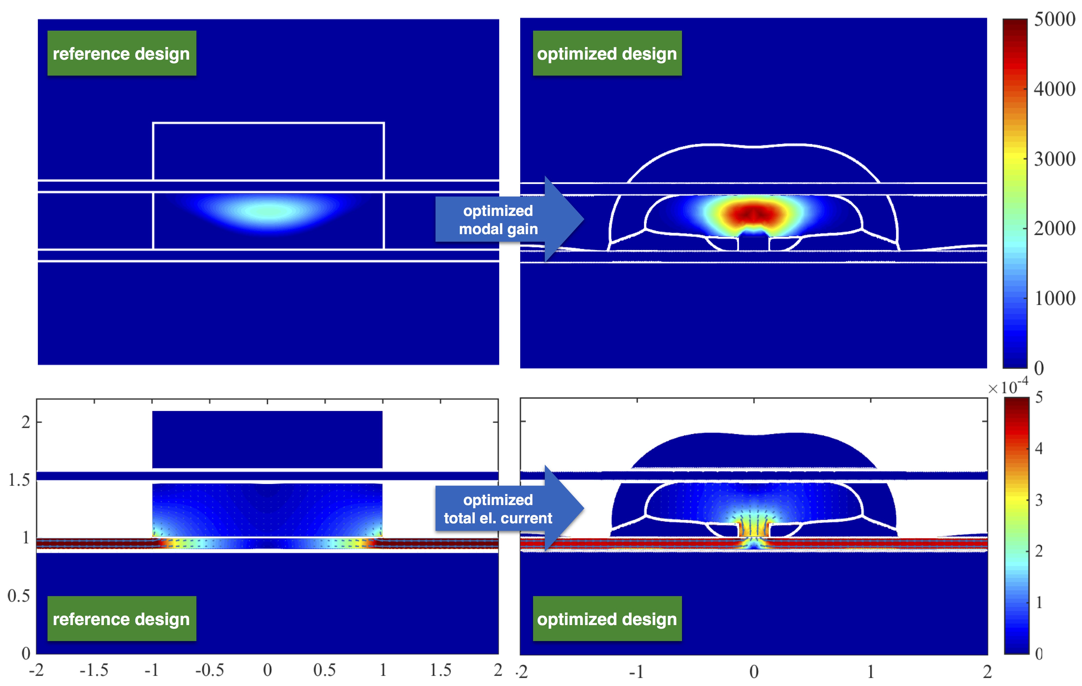
Figure 4: Different device topologies (left) reference microbridge (right) optimized microbridge cross section showing (top) modal gain and (bottom) electrical hole current computed after inserting doped Si contacts using artificial phase fields.
|
|
Publications
| [16] |
D. Peschka, Variational approach to contact line dynamics for thin films. WIAS preprint 2477, 2018
|
| [15] |
P. Farrell, D. Peschka, Challenges for drift-diffusion simulations of semiconductors: A comparative study of different discretization philosophies. WIAS preprint 2486, 2018
|
| [14] |
D. Peschka, N. Rotundo, and M. Thomas,
Doping optimization for optoelectronic devices.
Optical and Quantum Electronics, 50(3), 125, 2018
|
| [13] |
L. Adam, M. Hintermüller, T.M. Surowiec, A semismooth Newton method
with analytical path-following for the H1-projection onto the Gibbs
simplex WIAS preprint 2340, 2016
|
| [12] |
A. Mielke, D. Peschka, N. Rotundo, M. Thomas,
Gradient structure for optoelectronic models of semiconductors. WIAS
preprint 2340, Matheon preprint 1115, 2016, to appear in Proc. ECMI 2016
|
| [11] |
S. Hittmeir, J. Haskovec, P.A. Markowich, A. Mielke, Decay to equilibrium for energy reaction-diffusion systems,
Submitted, (Matheon
preprint, WIAS
preprint 2233, 2016).
|
| [10] |
M. Hintermüller and T. Surowiec, A nonsmooth approach for the optimal control of variational
inequalities of the second kind. Submitted to Comput. Optim. Appl., 2016.
|
| [9] |
M. Hintermüller and T. Surowiec, On the directional differentiability of the solution mapping for a class of variational inequalities of the second kind. Set-Valued and Variational Analysis, 1-12, 2017.
|
| [8] |
M. Hintermüller and T. Surowiec, A bundle-free implicit programming approach for a class of
elliptic MPECs in function space. Mathematical Programming 160.1-2: 271-305, 2016.
|
| [7] |
M. Hintermüller, T. Surowiec, and A. Kämmler, Generalized Nash equilibrium problems in Banach spaces: Theory, Nikaido-Isoda-based path-following methods, and applications. SIAM Journal on Optimization, 25(3):1826-1856, 2015.
|
| [6] |
D. Peschka, Numerics of contact line motion for thin films. IFAC, 48(1):390-393, 2015.
|
| [5] |
D. Peschka, N. Rotundo, and M. Thomas,
Towards doping optimization of semiconductor lasers,
(Journal of Computational and Theoretical Transport 45, pp. 410-423, 2016), (WIAS-Preprint 2180, Matheon preprint).
|
| [4] |
T. Koprucki, D. Peschka, M. Thomas,
Towards the Optimization of On-chip Germanium Lasers.
In: WIAS Annual Research Report 2015.
|
| [3] |
G. Capellini, M. Virgilio, Y. Yamamoto, L. Zimmermann, B. Tillack, D. Peschka, M. Thomas, A. Glitzky, R. Nürnberg, K. Gärtner,
Th. Koprucki, and Th. Schroeder, Modeling of an Edge-Emitting strained-Ge laser.
In: Proceedings of "Advanced Solid State Lasers 2015", OSA Publishing. 13(1):537-540.
|
| [2] |
D. Peschka, M. Thomas, A. Glitzky, R. Nürnberg, M. Virgilio, S. Guha, T. Schröder, G. Capellini, T. Koprucki,
Robustness analysis of a device concept for edge-emitting lasers based on strained germanium.
Topical Collection on "Numerical Simulation of Optoelectronic Devices, NUSOD'15",
Optical and Quantum Electronics Journal, 48:156, 2016. |
| [1] |
D. Peschka, M. Thomas, A. Glitzky, R. Nürnberg, K. Gärtner, M. Virgilio, S. Guha, T. Schröder, G. Capellini, T. Koprucki, Modeling of edge-emitting lasers based on tensile strained germanium microstripes.
IEEE Photonics Journal, 7 (2015) Art.-Id 1502115 |
|
Further references
| [R1] |
Bandelow, Gajewski, and Hünlich. Fabry-Perot lasers: Thermodynamics-based modeling. Optoelectronic Devices. Springer New York (2005). |
| [R2] |
Virgilio, Manganelli, Grosso, Pizzi, and Capellini, Radiative recombination and optical gain spectra in biaxially strained n-type germanium. Physical Review B (2013). |
[R3] |
Capellini, Reich, Guha, Yamamoto, Lisker, Virgilio, Ghrib, Kurdi, Boucaud, Tillack, and Schröder, Tensile Ge microstructures for lasing fabricated by means of a silicon complementary metal-oxidesemiconductor
process. Optics Express (2014) |
|
Presentations
- May 21-25, 2018: 9th International Conference ``Inverse Problems: Modeling and Simulation'' (IPMS 2018),
Malta; (M. Thomas)
Invited Talk: Optimization of the radiative emission for mechanically strained optoelectronic
semiconductor devices.
- March, 2018, 89th GAMM Annual Meeting, Munich; (D. Peschka)
Talk: Droplet and satellite droplet shedding in dewetting polymer films
- July 24-28, 2017, NUSOD 2017, Copenhagen; (D. Peschka)
Talk: Doping optimization for optoelectronic devices
- March 20-25, 2017, ICERM Workshop, Providence; (D. Peschka)
Invited Talk: Motion of thin droplets over surfaces
- July 18-22, 2016: 7ECM, Berlin, Germany;
Talk (CS-08-A): Analysis and optimization for edge-emitting
semiconductor-heterostructures. (M. Thomas)
Talk (MS-29-C): Coupling rate-independent and rate-dependent processes:
Existence results. (M. Thomas)
Talk (MS-29-C): A free boundary problem for the motion of viscous
liquids. (D. Peschka)
-
July 01-05, 2016: AIMS 2016, Orlando, Florida, USA; (M. Thomas)
Invited Talk (SS-02): Analysis and optimization for edge-emitting semiconductor-heterostructures.
Talk (SS-68): From adhesive contact to brittle delamination in visco-elastodynamics.
-
June 10, 2016: Oberseminar 'Mathematik in den Naturwissenschaften',
University of Würzburg, Germany; (M. Thomas)
Invited Talk: Coupling rate-independent and rate-dependent processes:
Delamination models in visco-elastodynamics.
-
March 07-11, 2016: Joint Annual Meeting of GAMM and DMV, Braunschweig,
Germany; (M. Thomas)
Talk: Nonsmooth PDEs in material failure -- Towards dynamic fracture.
-
Feb.22-26, 2016: ERC-Workshop on Modeling Materials and Fluids using
Variational Methods (MoMatFlu), WIAS, Berlin;
Talk: From adhesive contact to brittle delamination in
visco-elastodynamics. (M. Thomas)
Talk: A free boundary problem for the flow of viscous
bilayers. (D. Peschka)
- June 13-17,
2016, ECMI 2016, Santiago de Compostela; (D. Peschka)
Talk: Towards the optimization of Ge microbridges
-
March 03-04, 2016, 9th Annual Meeting Photonic Devices, FU Berlin; (D. Peschka)
Talk: Towards the optimization of on-chip germanium lasers.
-
February 20, 2016, Workshop on Variational Analysis and Optimization,
Marianska, Czech Republic; (L. Adam)
Invited talk: A multi-material phase-field approach for the optimal design of a Ge-on-Si
microlaser.
- February 16-17, 2016, WIAS-Days, TU Berlin; (M. Thomas)
Talk:
Modeling, analysis, and optimization of germanium-lasers.
-
December 28, 2015, Shenyang Institute Of Automation,
Chinese Academy Of Sciences, China; (L. Adam)
Invited talk: Optimal design of a germanium-on-silicon laser.
- September 07-11, 2015, SAMM 2015: Materials with Discontinuities, U Stuttgart;
L. Adam, poster: Optimal design of a Ge-on-Si laser aperature via a multi-material phase field
approach.
- August 10-14, 2015, ICIAM 8th International Congress on Industrial and Applied Mathematics, Beijing (China);
M. Thomas, invited talk in minisymposium (MS-Mo-D-56):
Analysis for edge-emitting semiconductor heterostructures.
-
June 22, 2015, International Workshop From Open to Closed Loop Control, Graz, Austria;
M. Hintermüller, talk: Optimal Control of Multiphase Fluids and Droplets.
- June 13, 2015, ISMP 2015, Pittsburgh, PA, USA;
M. Hintermüller, talk: Non-Smooth Cahn-Hilliard/Navier-Stokes Problems.
- March 11-13, 2015, AMaSiS, WIAS Berlin;
M. Thomas, talk:
Modeling of edge-emitting lasers based on tensile strained Germanium microstripes.
-
February 19, 2015, MathMod 2015, TU Vienna, Austria;
D. Peschka, invited talk in MS10: Numerics of
Contact Line Motion for Thin Films.
-
February 17-18, 2015, WIAS-Days;
M. Thomas, talk: Germanium lasers: Towards the optimization of mechanical strains and doping.
-
January 2015, Bilevel Optimal Control, Heidelberg, Germany;
T. Surowiec, talk: Nonsmooth analysis and implicit programming approaches for optimal control problems
governed by variational inequalities of the �1rst and second kind.
-
December 08, 2014, WSA 2014, Rio de Janeiro;
M. Hintermüller, plenary talk: Optimal Control of the Cahn-Hilliard System with Non-Smooth
Homogeneous Energy
Densities.
-
December 04, 2014, Seminar Dünne Filme, Freie Randwertprobleme, TU Berlin;
D. Peschka, invited talk: Modeling of suspension flows and its benefit for undergraduate studies.
-
October 16, 2014, RICAM, Linz (Austria);
M. Hintermüller, invited talk: Shape and Topological Sensitivity Based Methods in Tomographic
Reconstruction and
Image Segmentation.
-
September 09, 2014, NHOC 2014, Cascais (Portugal);
M. Hintermüller, plenary talk: Generalized Nash Equilibrium Problems in Banach Spaces.
|
Organization of project-related minisymposia, schools, and workshops
- 20th ECMI 2018 (June): Minisymposium Multiple scales in electromagnetic devices - from quantum mechanical effects to circuit simulation in Budapest,
organized by N. Rotundo, P. Farrell, D. Peschka (all WIAS).
- 7th ECM 2016: Minisymposium Nonsmooth PDEs in the modeling damage,
delamination, and fracture at TU Berlin,
organized by M. Thomas, E. Rocca (all WIAS).
- 7th ECM 2016: Minisymposium Mathematical methods for semiconductors at TU Berlin,
organized by N. Rotundo, P. Farrell, D. Peschka (all WIAS).
- 11th AIMS Conference on Dynamical Systems, Differential Equations and
Applications (Orlando, US): Special Session Rate-dependent and
rate-independent evolution problems in continuum mechanics: Analytical and
numerical aspects.
organized by M. Thomas, G. Lazzaroni (SISSA Trieste)
- The 19th European Conference on Mathematics for Industry 2016: Minisymposium Charge transport in semiconductor materials: Emerging and established mathematical topics in Santiago de Compostela (Spain),
organized by N. Rotundo, P. Farrell, D. Peschka (all WIAS).
-
November 30-December 4, 2015: PDE2015 - Theory and Applications of Partial Differential Equations,
WIAS Berlin,
organized by H.-C. Kaiser, A. Mielke, J. Rehberg, E. Rocca, M. Thomas, E. Valdinoci (all WIAS), D. Knees (U Kassel).
-
July 07-11, 2015 SIAM Conference on Control and Its Applications, CT15: Minisymposium MS4 Optimal Control of Multiphase Systems,
organized by D. Wegner (HUB) and M. Hintermüller.
|