
This topic is currently not treated at the WIAS.
One option to for semiconductor device manufacturing is optical lithography. In this process, a pattern defined by a photomask is transferred by light into a photosensitive film (photoresist) by light. The photoresist processing steps for an exemplary pattern transferred into silicon dioxide on the top of a silicon wafer are sketched in the following picture.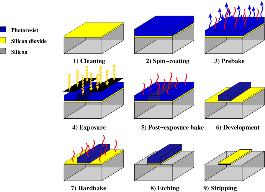
- Zoom Image: © 2007 T. Schnattinger
- Exposure:
During this step, the molecules of the Photo Acid Generator (PAG) hit by photons split off acid molecules. The obtained acid concentration is the input for the next process step. - Post-Exposure Bake (PEB):
Photogenerated acid acts as a catalyst for splitting polymer bonds. After a given time t PEB, the process step yields the concentration of the still existing polymer bonds, also called inhibitor concentration. The so-called meta-model, describes the the post exposure bake by a system of reaction diffusion equations: - fast acid base neutralization: A + B --> X AB,
- acid catalyzed inhibitor deprotection: A + M --> A + X M,
- diffusion of acid and base.
- Development:
During this step the deprotected resist regions are dissolved. - Etch:
Etching then creates structures in the blank parts of the substrate surface.
Highlights
 |  | | Therefore, the research network MD3 ”Material Development for Double exposure and Double patterning” funded by the Seventh EU Framework Programme (FP7), a number of process options for the 32 nm technological node have been investigated with respect to their technological and economical feasibility. |
Publications
 Articles in Refereed Journals
-
A. Fiebach, A. Glitzky, A. Linke, Convergence of an implicit Voronoi finite volume method for reaction-diffusion problems, Numerical Methods for Partial Differential Equations. An International Journal, 32 (2016), pp. 141--174.
Abstract
We investigate the convergence of an implicit Voronoi finite volume method for reaction- diffusion problems including nonlinear diffusion in two space dimensions. The model allows to handle heterogeneous materials and uses the chemical potentials of the involved species as primary variables. The numerical scheme uses boundary conforming Delaunay meshes and preserves positivity and the dissipative property of the continuous system. Starting from a result on the global stability of the scheme (uniform, mesh-independent global upper and lower bounds), we prove strong convergence of the chemical activities and their gradients to a weak solution of the continuous problem. In order to illustrate the preservation of qualitative properties by the numerical scheme, we present a long-term simulation of the Michaelis-Menten-Henri system. Especially, we investigate the decay properties of the relative free energy and the evolution of the dissipation rate over several magnitudes of time, and obtain experimental orders of convergence for these quantities. -
A. Fiebach, A. Glitzky, A. Linke, Uniform global bounds for solutions of an implicit Voronoi finite volume method for reaction-diffusion problems, Numerische Mathematik, 128 (2014), pp. 31--72.
Abstract
We consider discretizations for reaction-diffusion systems with nonlinear diffusion in two space dimensions. The applied model allows to handle heterogeneous materials and uses the chemical potentials of the involved species as primary variables. We propose an implicit Voronoi finite volume discretization on regular Delaunay meshes that allows to prove uniform, mesh-independent global upper and lower $L^infty$ bounds for the chemical potentials. These bounds provide the main step for a convergence analysis for the full discretized nonlinear evolution problem. The fundamental ideas are energy estimates, a discrete Moser iteration and the use of discrete Gagliardo-Nirenberg inequalities. For the proof of the Gagliardo-Nirenberg inequalities we exploit that the discrete Voronoi finite volume gradient norm in $2d$ coincides with the gradient norm of continuous piecewise linear finite elements. -
J. Fuhrmann, A. Fiebach, A. Erdmann, P. Trefonas, Acid diffusion effects between resists in freezing processes used for contact hole patterning, Microelectronic Engineering, 87 (2010), pp. 951--954.
Abstract
Double patterning following an litho?litho-etch scheme is a possible option to create structure widths below the nominal resolution of optical light with current exposure technology. Interactions between the first and second resist layers may influence the final structure created. In this paper, we perform a model based investigation of the possible consequences of the diffusion of photo-generated acid from the second resist to the first one. As a consequence, less acid is available for the deprotection reaction, and we observe a tendency to an increase of the CD values of the primary structure. We attempt to explain observed footing effects in contact holes by this effect. -
J. Fuhrmann, A. Erdmann, Ch.R. Szmanda, A. Fiebach, M. Uhle, A model of self-limiting residual acid diffusion for pattern doubling, Microelectronic Engineering, 86 (2009), pp. 792--795.
Contributions to Collected Editions
-
A. Erdmann, F. Shao, J. Fuhrmann, A. Fiebach, G.P. Patsis, P. Trefonas, Modeling of double patterning interactions in litho-cure-litho-etch (LCLE) processes, in: Optical Microlithography XXIII, Part I, M.V. Dusa, W. Conley, eds., 7640 of Proceedings of SPIE, SPIE, 2010, pp. 76400B/1--76400B/12.
Abstract
This paper uses advanced modeling techniques to explore interactions between the two lithography processes in a lithocure- etch process and to qualify their impact on the final resist profiles and process performance. Specifically, wafer topography effects due to different optical properties of involved photoresist materials, linewidth variations in the second lithography step due to partial deprotection of imperfectly cured resist, and acid/quencher diffusion effects between resist materials are investigated. The paper highlights the results of the simulation work package of the European MD3 project. -
J. Fuhrmann, A. Fiebach, G.P. Patsis, Macroscopic and stochastic modeling approaches to pattern doubling by acid catalyzed cross-linking, in: Advances in Resist Materials and Processing Technology XXVII, Part I, R.D. Allen, M.H. Somervell, eds., 7639 of Proceedings of SPIE, SPIE, 2010, pp. 76392I/1--76392I/9.
Abstract
Pattern doubling by cross-linking of a spacer triggered by residual acid diffusion from a previously developed primary structure into the spacer is a possible option to create structure widths below the nominal resolution of the optical process. An advantage of such a process step would be the self-alignment to the primary structure, which would render a second exposure step unnecessary. Using macroscopic and stochastic modeling approaches, we demonstrate that it may be possible to control the width of the secondary structure created by cross-linking by the amount of quencher base added.
Talks, Poster
-
O. Marquardt, Nucleation chronology and electronic properties of In(As,Sb,P) graded-composition quantum dots (online talk), NUSOD 2020: 20th International Conference on Numerical Simulation of Optoelectronic Devices (Online Event), September 14 - 25, 2020, Politecnico di Torino, September 14, 2020.
-
O. Marquardt, Nucleation chronology and electronic properties of In(As,Sb,P) graded-composition quantum dots (online talk), CMD2020GEFES (Online Event), August 31 - September 4, 2020, European Physical Society & La Real Sociedad Española de Física, September 4, 2020.
-
A. Fiebach, A. Glitzky, K. Gärtner, A. Linke, Voronoi finite volume methods for reaction-diffusion systems, MoMaS Multiphase Seminar Days --- Journées MoMaS Multiphasiques, Bures-sur-Yvette, France, October 7 - 9, 2013.
-
A. Fiebach, A. Glitzky, A. Linke, Voronoi finite-volume methods for reaction-diffusion-systems, 33. Norddeutsches Kolloquium über Angewandte Analysis und Numerische Mathematik (NoKo 2012), Universität Rostock, Institut für Mathematik, May 4 - 5, 2012.
-
A. Fiebach, Problems in double patterning: resist footing, The 16th European Conference on Mathematics for Industry (ECMI 2010), July 26 - 30, 2010, Bergische Universität Wuppertal, July 27, 2010.
-
J. Fuhrmann, A. Fiebach, G.P. Patsis, Macroscopic and stochastic modeling approaches to pattern doubling by acid catalyzed cross-linking, Workshop ``SPIE Advanced Lithography'', San Jose, California, USA, February 21 - 25, 2010.
-
K. Gärtner, Charge explosion simulations, 7th Meeting of the Detector Advisory Committee for the European XFEL, European XDAC, Hamburg, May 26, 2010.
-
K. Gärtner, Plasma effects --- Status of simulations (10'), 8th Meeting of the Detector Advisory Committee for the European XFEL, European XDAC, Hamburg, November 15, 2010.
-
A. Fiebach, J. Fuhrmann, Numerical issues for reaction-diffusion processes in semiconductor photoresists, Workshop ``Evolution Equations, Related Topics and Applications'', München, September 7 - 11, 2009.
-
J. Fuhrmann, A. Fiebach, A. Erdmann, P. Trefonas, Acid diffusion effects between resists in freezing processes used for contact hole patterning, 35th International Conference on Micro and Nano Engineering (MNE 2009), Ghent, Belgium, September 29 - 30, 2009.
-
J. Fuhrmann, Modeling and simulation of post exposure bake processes in double patterning, 7th Fraunhofer IISB Lithography Simulation Workshop, September 25 - 27, 2009, Hersbruck, September 26, 2009.
-
J. Fuhrmann, Reaction-diffusion processes in polymer resists, Workshop ``Evolution Equations, Related Topics and Applications'', September 7 - 11, 2009, Helmholz-Zentrum München, September 8, 2009.
-
A. Fiebach, PE-simulation: Benchmarking of numerical solvers for 2D and 3D geometries, 6th Fraunhofer IISB Lithography Simulation Workshop, September 19 - 20, 2008, Athen, Greece, September 19, 2008.
-
A. Fiebach, J. Fuhrmann, Some reaction diffusion problems in semiconductor device fabrication, Workshop on PDE Approximations in Fast Reaction -- Slow Diffusion Scenarios, Leiden, Netherlands, November 10 - 14, 2008.