Collaborator: U. Bandelow
(FG 1),
Th. Koprucki
(FG 3)
Supported by: DFG: Priority Program ,,Analysis,
Modellbildung und Simulation von Mehrskalenproblemen``
(Analysis, modeling and simulation of multiscale problems)
Description:
Eight-band kp-Hamiltonians [1]
are detailed models for the calculation of quantum-confined
states in semiconductor quantum-well
structures,
because they consistently include band mixing, spin-orbit interaction and
strain effects. Quantities such as carrier densities
or the optical response can be efficiently obtained in terms of the states
([2]).
To utilize such microscopically calculated data for device simulation,
e.g., with drift-diffusion-type models [2],
[3], a suitable
upscaling to macroscopic state equations is required.
We have demonstrated upscaling schemes for the carrier densities,
the peak gain characteristics and the spontaneous radiative
recombination rate calculated with WIAS-QW for an example
quantum-well structure [3].
The investigations have been carried out for
an InGaAsP-based single quantum-well structure which
is designed for emission at 1.55  consisting
of a compressively strained quantum well
of width dQW=7 nm sandwiched between tensile strained barriers.
consisting
of a compressively strained quantum well
of width dQW=7 nm sandwiched between tensile strained barriers.
As a first example for upscaling we consider the carrier densities.
kp calculations [2]
generically provide local carrier densities n(z) and p(z)
depending on the Fermi levels Fe and Fh
and the temperature T. Since the carriers localize very well
in the quantum well [2] we can introduce an
average carrier density per quantum well
 as a natural quantity for upscaling.
Thus we obtain from the microscopical model the relations
as a natural quantity for upscaling.
Thus we obtain from the microscopical model the relations  and
and  for the averaged carrier densities as depicted
in Figure 1. The upscaling to a macroscopic level
can then be performed by fitting the calculated relations
and to
macroscopic state equations such as the Fermi distribution
used in drift-diffusion models. As shown in Figure 1
we observed that both quantities can be reasonably fitted to the relations
for the averaged carrier densities as depicted
in Figure 1. The upscaling to a macroscopic level
can then be performed by fitting the calculated relations
and to
macroscopic state equations such as the Fermi distribution
used in drift-diffusion models. As shown in Figure 1
we observed that both quantities can be reasonably fitted to the relations
| 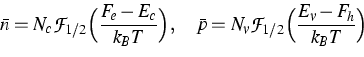 |
(1) |
by adjusting the effective band edges Ec and Ev and the
band-edge densities of state Nc and Nv.  is
the Fermi integral of order 1/2. The fit for the valence bands is
very close to the calculated curve for a wide range of densities and
temperatures whereas for the conduction bands the macroscopic
state equation yields a good approximation only
for a certain range of parameters.
Thus, an upscaling of band-structure information by the dependence of
the average density per quantum well on the Fermi level is possible.
This allows us to treat the quantum well as a classical material
with microscopically defined band-edge densities of state Nc and Nv
and net band edges Ec and Ev which
differ from the band-structure parameters of the well material
and cannot be estimated elsewhere.
is
the Fermi integral of order 1/2. The fit for the valence bands is
very close to the calculated curve for a wide range of densities and
temperatures whereas for the conduction bands the macroscopic
state equation yields a good approximation only
for a certain range of parameters.
Thus, an upscaling of band-structure information by the dependence of
the average density per quantum well on the Fermi level is possible.
This allows us to treat the quantum well as a classical material
with microscopically defined band-edge densities of state Nc and Nv
and net band edges Ec and Ev which
differ from the band-structure parameters of the well material
and cannot be estimated elsewhere.
Fig. 1:
Relation between the average carrier densities
 and the Fermi levels Fe,Fh
relative to the net band edge Ec, Ev for the temperatures
T=290 K, 315 K, 340 K. The dashed lines indicate
the fit to the macroscopic state equation (1). Left: electrons occupying
the conduction subbands, right: holes occupying the valence subbands.
and the Fermi levels Fe,Fh
relative to the net band edge Ec, Ev for the temperatures
T=290 K, 315 K, 340 K. The dashed lines indicate
the fit to the macroscopic state equation (1). Left: electrons occupying
the conduction subbands, right: holes occupying the valence subbands.
![\makeatletter
\@ZweiProjektbilderNocap[h]{0.45\textwidth}{fit_3ddos_cb}{fit_dos_vb}
\makeatother](img528.gif)
|
Furthermore, the spectra of the optical material gain can
be calculated in terms of the band-structure and
transition matrix elements given by the wavefunctions
[2], [3]. This
defines a function  depending on the transition energy
 , the Fermi levels Fe and Fh
and the temperature T.
Most lasers are designed to emit at the spectral gain maximum.
Therefore the peak gain gp is an important quantity.
, the Fermi levels Fe and Fh
and the temperature T.
Most lasers are designed to emit at the spectral gain maximum.
Therefore the peak gain gp is an important quantity.
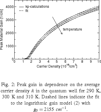
As a second example we have calculated the peak gain  (assuming charge neutrality
 =
= ) as a function of the average carrier
density introduced above. The result is depicted in
Figure 2. For sufficiently high
carrier densities (above
) as a function of the average carrier
density introduced above. The result is depicted in
Figure 2. For sufficiently high
carrier densities (above  )
this peak gain characteristics can be upscaled to
a usually used state equation given by the logarithmic gain model
)
this peak gain characteristics can be upscaled to
a usually used state equation given by the logarithmic gain model
| 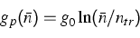 |
(2) |
as shown in Figure 2. However, for low densities this
way of upscaling completely fails. The constant g0 appears
to be nearly independent of the temperature whereas the transparency
carrier density ntr should roughly linearly increase with
the temperature.
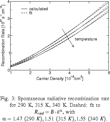
As a third example we analyzed the upscaling of the spontaneous
radiative recombination rate [3]
which is a further important quantity
for the analysis of semiconductor lasers, because it essentially
determines the laser threshold.
The spontaneous radiative recombination rate Rrad(Fe, Fh, T)
obtained by the kp calculations depends
on the Fermi levels Fe and Fh and the temperature.
Again, for local charge neutrality  we found out that this relation can
be suitably upscaled to the power law
we found out that this relation can
be suitably upscaled to the power law
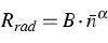
as depicted in Figure 3. The exponent for the fit
was approximately  , which differs from the
commonly used models corresponding to
, which differs from the
commonly used models corresponding to  .
.
References:
- U. BANDELOW, H.-CHR. KAISER, TH. KOPRUCKI,
J. REHBERG, Spectral properties of
 Schrödinger operators in one
space dimension, Numer. Funct. Anal.
Optim., 21 (2000), pp. 379-409.
Schrödinger operators in one
space dimension, Numer. Funct. Anal.
Optim., 21 (2000), pp. 379-409.
-
 , Modeling and simulation of strained quantum
wells in semiconductor lasers,
to appear in: Mathematics --
Key Technology for the Future II,
K.-H. Hoffmann, W. Jäger, T. Lohmann,
H. Schunck, eds.,
Springer, Berlin, Heidelberg.
, Modeling and simulation of strained quantum
wells in semiconductor lasers,
to appear in: Mathematics --
Key Technology for the Future II,
K.-H. Hoffmann, W. Jäger, T. Lohmann,
H. Schunck, eds.,
Springer, Berlin, Heidelberg.
- U. BANDELOW, R. HÜNLICH,
TH. KOPRUCKI, Simulation of
static and dynamic properties of
edge-emitting multi quantum well lasers,
WIAS Preprint no. 799
, 2002.
LaTeX typesetting by I. Bremer
5/16/2003