|
|
|
[Contents] | [Index] |
Supported by: DFG: Priority Program ``Analysis, Modellierung und Simulation von Mehrskalenproblemen'' (Analysis, modeling and simulation of multiscale problems)
Description: Although diode lasers have existed for more than 25 years, blue-emitting diodes have only recently been realizable. This closed the ``gap'' between devices emitting in the visible spectral range and gives rise to many applications with a big market potential. Such applications include active laser tv, increasing storage capacities on DVDs and very high-quality laser printers.
The technological breakthrough to the blue laser diodes came with the successful epitaxy of GaN-based nanostructures. Typically, these materials grow in crystallographic wurtzite configurations and display a large energy band gap, as well as other unusual features.
We have simulated such nanostructures using
the eight-band kp-model for wurtzite semiconductors
in WIAS-QW.
This model is a generalization of [1] including strain,
spin-orbit interaction, and crystal-field splitting.
A primary result of such kp-calculations
is the subband structure (dependence of the energy
on the in-plane wave vector ![]() ),
as depicted in Fig. 1.
),
as depicted in Fig. 1.
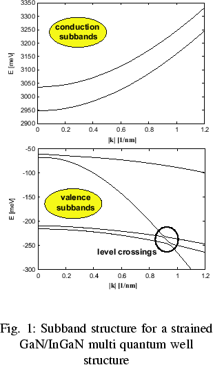 As shown in Fig. 1, the subband structure exhibits
some remarkable properties, which partially differ from those
known from other laser materials:
As shown in Fig. 1, the subband structure exhibits
some remarkable properties, which partially differ from those
known from other laser materials:
Furthermore, eight-band kp-calculations allow for a realistic prediction
of the matrix elements for the optical
interband transitions ([3]), which are
a prerequisite for the calculation of the optical response function for
such nanostructures.
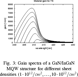 As a representation for the imaginary part of the optical response function,
we have calculated the spectra of the optical material gain
(TE-polarization has been assumed) for different sheet densities,
as illustrated in Fig.2.
The gain increases monotonically with the carrier density,
but much higher densities are required for the laser threshold,
compared to other semiconductor materials.
This is mainly due to the much higher effective masses in GaN-based materials,
as discussed above, but in some part also due to the reduced interband
mixing.
As a representation for the imaginary part of the optical response function,
we have calculated the spectra of the optical material gain
(TE-polarization has been assumed) for different sheet densities,
as illustrated in Fig.2.
The gain increases monotonically with the carrier density,
but much higher densities are required for the laser threshold,
compared to other semiconductor materials.
This is mainly due to the much higher effective masses in GaN-based materials,
as discussed above, but in some part also due to the reduced interband
mixing.
Pure kp-calculations correspond to the exclusion of any Coulomb interaction between the carriers. Being charged fermions, their behavior can be drastically modified by such Coulomb effects. In particular, such impacts have been studied for GaN/InGaN quantum wells ([2]).
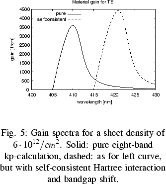 For the calculation of some prominent Coulomb effects, we used a
Kohn-Sham type model similar to [3],
which has already been successfully
applied to analyzing InP-based nanostructures.
It includes the Hartree contribution via the Poisson equation
and the bandgap shift via exchange-correlation potentials.
As a result of such self-consistent calculations,
the gain spectra experience a density-dependent red shift
and a small enhancement, as observed by the difference between
the curves in Fig.3.
In addition, the electrons become more strongly confined, whereas
the holes stay untouched in the self-consistent case.
This is in contrast to the situation of InP-based nanostructures
([3])
and can be explained by the large heavy hole mass.
For the calculation of some prominent Coulomb effects, we used a
Kohn-Sham type model similar to [3],
which has already been successfully
applied to analyzing InP-based nanostructures.
It includes the Hartree contribution via the Poisson equation
and the bandgap shift via exchange-correlation potentials.
As a result of such self-consistent calculations,
the gain spectra experience a density-dependent red shift
and a small enhancement, as observed by the difference between
the curves in Fig.3.
In addition, the electrons become more strongly confined, whereas
the holes stay untouched in the self-consistent case.
This is in contrast to the situation of InP-based nanostructures
([3])
and can be explained by the large heavy hole mass.
References:
|
|
|
[Contents] | [Index] |