The project's timespan is 01.01.2023- 31.03.2026, whereas WIAS starts on
01.04.2023. The main aims of the project are modeling and design (FBH+WIAS),
as well as fabrication and characterization (FBH) of novel high-power Photonic
Crystal Surface Emitting Laser (PCSEL) devices. This will be achieved by
combining the expertise of the cooperation partners in semiconductor laser
modeling, design, fabrication, and characterization.
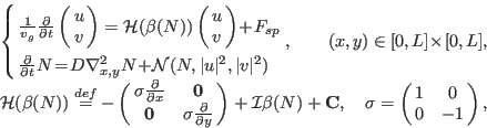
Semiconductor diode lasers are small, efficient, and relatively cheap devices used in many modern applications. Multiple applications require emission powers exceeding several ten Watts from a single diode and up to a few kiloWatts from a combined laser system. In this project, we consider novel Photonic Crystal Surface-Emitting Lasers (PCSELs), which, in contrast to conventional high-power edge-emitting broad-area lasers (BALs), are capable of emitting high power (up to 80 W at the moment [Inoue 2023]) beams of nearly perfect quality in the (z) direction, perpendicular to the (x/y) plain of active material. The critical part of PCSELs, enabling an efficient coupling of within the active layer generated optical fields and their redirection along the z axis, is a properly constructed 2-dimensional photonic crystal layer. In simple cases, this PC layer can be vertically homogeneous or consist of several vertically homogeneous layers (e.g., three layers as shown in Figure 1). In many more general cases, when the borders of the PC features are not vertical, the whole PC layer still can be reasonably well approximated by multiple very thin vertically homogeneous layers.
The initial model to be considered and integrated numerically [Inoue 2019] is derived from Maxwell equations and is a 1 (time)+2 (space) dimensional system of PDEs for complex optical fields u(t,x,y)=(u+,u-)T, v(t,x,y)=(v+,v-)T, and real carrier density N(t,x,y):
whereas the complex field functions u± and v± satisfy boundary conditions (BCs) Besides, an efficient location of several leading modes (Ω,Θ) of the related spectral problem [Liang 2012], defined by a system of four 2-D PDEs, is of great importance when designing PCSEL devices.Several significant challenges arising when treating the above-stated problems are a nontrivial construction of the implicitly defined 4×4 field coupling matrix C, requiring a solution of the Helmholtz problem and multiple integrations of the calculated mode profile with different separately constructed exponentially growing and decaying Green's functions, as well as simulations and (spectral) analysis of large discrete problems relating up to several million variables in large-emission-area (large L) PCSELs.
In the frame of the PCSELence project, we have developed analytic-expression-based algorithms for the construction of the field coupling matrix C entering model equations (1) and (3). Our algorithms bypass computer arithmetic-induced problems when dealing with large and small exponentials; they are fast and exact, in contrast to approximative approaches or procedures based on numerical integration methods [1,2,3]. An efficient calculation of leading optical modes in PCSELs is crucial when looking for suitable heterostructures including size and configuration of lateral photonic crystal layers. Our algorithms and the numerical solver can be also explored to consider PCSELs with multiple photonic crystal layers and large emission areas. Such calculations are beneficial when looking for PCSEL designs with low thresholds and good main mode gain separation, which is crucial when seeking a single-mode high-quality emission. Moreover, our solver can also be used to predict an intrinsic linewidth if the stable single-mode operation of PCSEL is ensured [4].
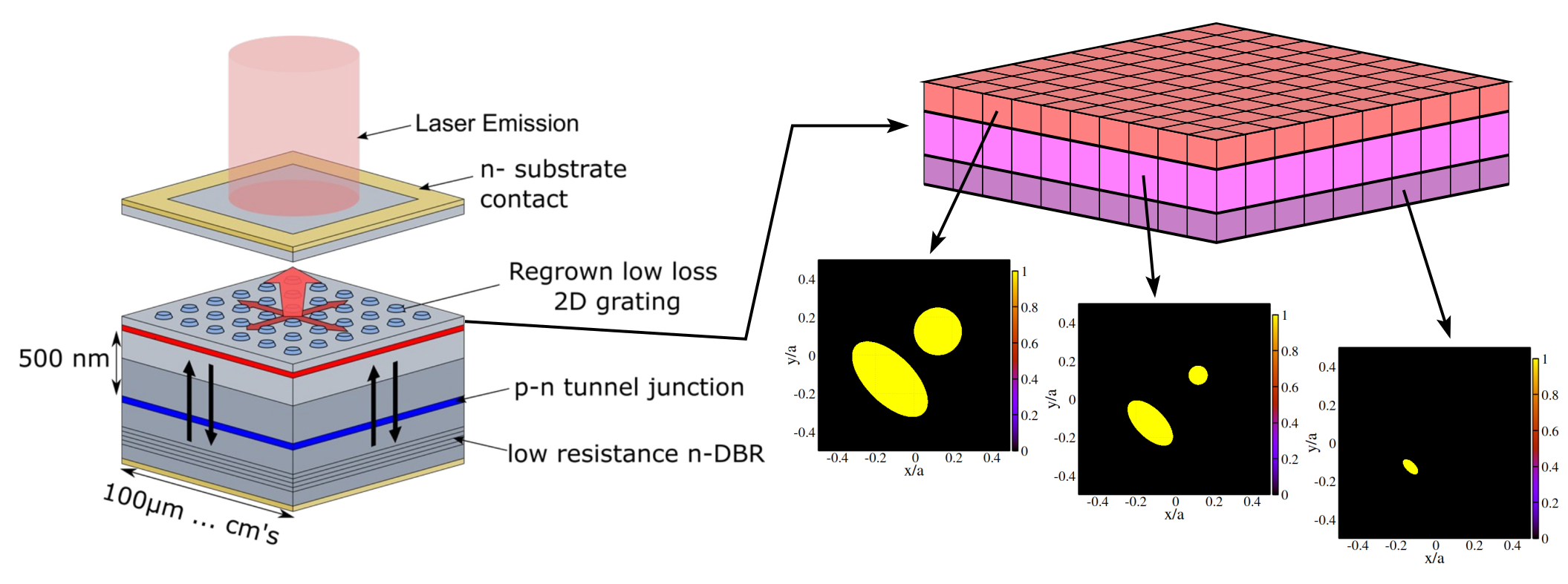
There are at least two sources of errors in calculating the eigenvalues of the spectral problem. One source of these errors is related to the nature of the coupling matrix C, which, in general, is defined as an infinite sum of submatrices, each constructed using specific Fourier coefficients of the refractive index expansion in the PC layer. In practical calculations, one has to truncate this sum, keeping only about D2 submatrices. Fortunately, our effective algorithms allow fast estimation of these submatrices, such that typically, the matrix C can be calculated with a high precision factor D=500 within a fraction of a minute: see Figs. 2a,b, where changes in the matrix elements and the eigenvalues with the increasing number of submatrices in this infinite sum are shown. For more details, see Ref. [3].
The numerical discretization of the problem induces another source for errors in calculated leading eigenvalues. In general, numerical approaches do not allow the finding of all (an infinite number!) eigenvalues of the continuous spectral problem. Fortunately, in practical applications, only several or several-tenths of eigenvalues are essential, and these eigenvalues can be found with pretty high precision when using relatively coarse numerical meshes. We also apply the higher-order numerical schemes to improve the accuracy: see Figs. 2d,e, presenting a study of numerical errors of two leading eigenvalues in dependence on the mesh's roughness and the scheme's precision order. Panel c of the same figure shows the time required to calculate five leading eigenvalues. For more details, see Ref. [2].
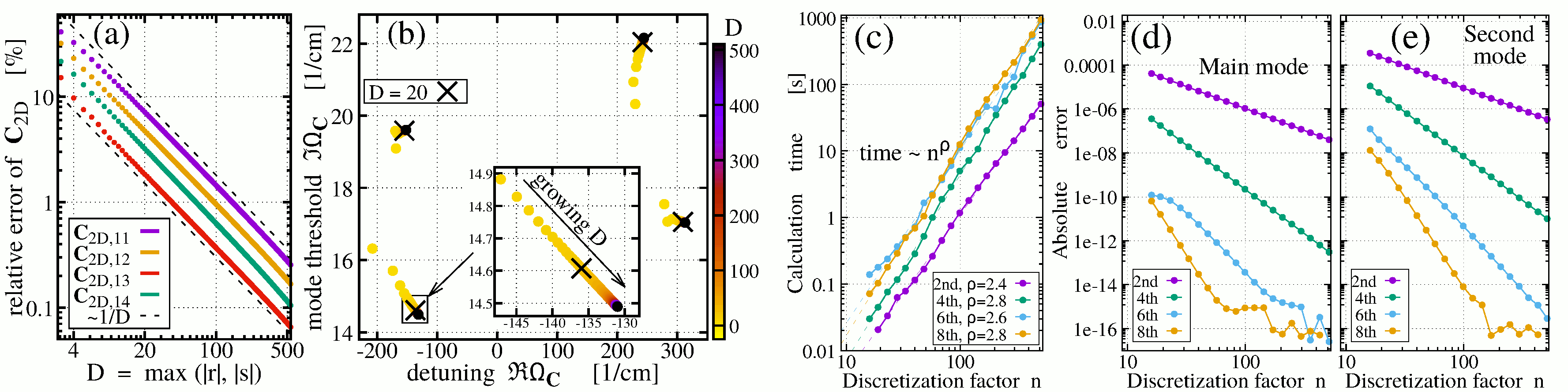
Fig. 3 shows an example of the calculated spectra of a particular PCSEL device. In panel (a), we calculate the most important modes of the discretized spectral problem (3) (small light-blue dots), compare their eigenvalues to those of two limit-case problems (large full triangles and red squares or rhombs), and inspect spatial distributions of five main modes at the right-hand side of the panel. These simulations are performed for fixed L= 1 mm. It is crucial to minimize the imaginary part of Ω (i.e., to reduce the threshold gain and bias current required to achieve the lasing), increase the separation between ImΩ of two principal modes (which is needed for achieving a single-mode lasing), and minimize the contribution of mode intensity at the lateral borders of PCSEL (which allows to reduce field losses αe at these boundaries). Panel (b) of the same figure shows changes of above-mentioned characteristics with increasing L. Such parameter scan calculations are very useful when looking for suitable PCSEL configurations.
For further information please contact
Dr. Mindaugas Radziunas
Weierstrass-Institute for Applied
Analysis and Stochastics
Mohrenstrasse 39
10117 Berlin
Tel.: (030) 20372-441
Fax : (030) 2044975
E-mail: radziunas@wias-berlin.de
WWW: http://www.wias-berlin.de