|
|
|
[Contents] | [Index] |
Collaborator: H. Gajewski (FG 1), R. Nürnberg (FG 1), G. Schmidt (FG 4)
Cooperation with: CiS Institut für Mikrosensorik gGmbH, Erfurt; Silicon Sensor International AG, Berlin
Description: The project is concerned with the mathematical modeling and numerical simulation of optoelectronical semiconductor sensors for microsystem technology. Optical sensors and radiation detectors play an important role in robot engineering, material science, and many other areas of modern technology. And semiconductor structures are ideally suited for converting incoming information such as light, X-rays, or particle radiation into an electrical signal.
A simultaneous mathematical modeling of light diffusion and absorption as well as charge generation and transport is needed for both the physical understanding and the optimization of optical semiconductor detectors. An adequate model consists of Maxwell equations for the optical processes and drift-diffusion and heat flow equations for the electronical processes. These equations are coupled via optical, avalanche, and thermal source terms.
The aim of the project was to extend and further develop the simulation program WIAS-TeSCA with regard to new requirements in the development of these devices. This included the analytical foundation, implementation, and testing of efficient solution algorithms for the coupled system of equations. The results will be evaluated with the help of real-life optical sensors, namely position sensors and avalanche photodiodes, taken from the manufacturing line of our project partners.
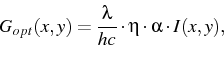
The main focus of the project was on the integration of a module to calculate light diffusion in structured optical films into the device simulation tool WIAS-TeSCA. The interaction between light rays and charge transport is modeled with the generation rates in the corresponding partial differential equations. This optical charge generation is described with the ansatz
where ![]() is the wavelength of incoming light,
is the wavelength of incoming light,
![]() is the quantum efficiency,
is the quantum efficiency, ![]() is the absorption constant.
The intensity I of the electromagnetic field depends on the optical and
geometric characteristics of the structure and on properties of the
incoming light, such as spectral distribution, polarization, coherence, and
contact angle. Since the wavelength is comparable with the dimensions
of relevant sensors, diffraction effects come into play. Hence, geometrical optics
approaches are no longer sufficient and the light intensity has to be obtained
as a solution of the time-harmonic Maxwell equation.
Under assumptions of constant permeability
is the absorption constant.
The intensity I of the electromagnetic field depends on the optical and
geometric characteristics of the structure and on properties of the
incoming light, such as spectral distribution, polarization, coherence, and
contact angle. Since the wavelength is comparable with the dimensions
of relevant sensors, diffraction effects come into play. Hence, geometrical optics
approaches are no longer sufficient and the light intensity has to be obtained
as a solution of the time-harmonic Maxwell equation.
Under assumptions of constant permeability ![]() and
of the invariance of the structure
in z direction, but oblique incidence of the plane electromagnetic waves
e i(
and
of the invariance of the structure
in z direction, but oblique incidence of the plane electromagnetic waves
e i(![]() x-
x-![]() y+
y+![]() z)+i
z)+i![]() t, that are
valid here, this equation can be reduced to a system of two-dimensional
Helmholtz equations.
More precisely,
the z components of the electromagnetic field have the form
Ez(x, y)e i
t, that are
valid here, this equation can be reduced to a system of two-dimensional
Helmholtz equations.
More precisely,
the z components of the electromagnetic field have the form
Ez(x, y)e i![]() z,
Hz(x, y)e i
z,
Hz(x, y)e i![]() z and
the functions Ez, Hz satisfy the Helmholtz equations
z and
the functions Ez, Hz satisfy the Helmholtz equations
 |
To solve the Helmholtz equations, we make use of the program DiPoG which was developed at WIAS to simulate and optimize periodic diffraction gratings, [6], and was enlarged for this application. The program is based on the Finite Element Method and the forward solver calculates the efficiency of gratings under conical incidence of plane electromagnetic waves. In order to integrate this module into the program WIAS-TeSCA, we, in particular, implemented an efficient method to model thick layers inside the optical structure, different routines to postprocess the calculated field distributions and an effective exchange of the field and intensity distributions, inside the semiconductor structure.
For the project partner CiS, we have successfully simulated a position sensor.
In this case, there are several optical layers on the CiS photodiode,
two of which have a chrome strip and can be moved against each other.
As the structure's dimensions are within a few ![]() m, the light diffusion
in the optical grid is determined by diffraction effects.
The computed entities are the characteristics of the photodiode, the
photocurrent with fixed voltage depending on the lateral translations of the
structured layers with respect to each other.
m, the light diffusion
in the optical grid is determined by diffraction effects.
The computed entities are the characteristics of the photodiode, the
photocurrent with fixed voltage depending on the lateral translations of the
structured layers with respect to each other.
When the sensor is used in practice, the incoming light is not monochromatic and
its angle varies depending on the used optics. That is why a whole bundle of
rays that sufficiently describes the spectral distribution and the angle
variation has to be used in the optical simulation.
Solving the Helmholtz equation, the spatial and temporal coherence cannot
be accounted for by simply using correction coefficients.
Hence, the computational expense increases considerably.
In relevant test examples (a Gaussian spectral distribution with a
half band width of 40 nm and an angle variation of
![]() 1o),
computational costs for a ``mean'' characteristic curve are
similar to the costs for 100 single ones, in order to obtain practically
usable and stable results.
Note that in order to compute a single characteristic curve,
the optical equations had to be solved about 30 times.
1o),
computational costs for a ``mean'' characteristic curve are
similar to the costs for 100 single ones, in order to obtain practically
usable and stable results.
Note that in order to compute a single characteristic curve,
the optical equations had to be solved about 30 times.
The above-mentioned demands illustrate why we have focused on making our simulation software highly efficient. In particular, this covers the appropriate choice of grids for the structured optical layers as well as the effective organization of variations in the geometry (lateral translations), in the wavelength and in the angle of incidence.
The following figures show the dependence of the displacement characteristics on the wavelength and the angle of the incoming light.
![\makeatletter
\@ZweiProjektbilderNocap[h]{0.46 \textwidth}{cis-var-d130-l880me.eps}{cis-var-d130-w0me.eps}
\makeatother](img860.gif) |
The characteristics for spatially and temporally scattered light enabled us
to predict the effect of varying the layer structure and of coating
the chrome strips. In this coating example, the modulation depth increased
by approximately 25 %.
![\makeatletter
\@ZweiProjektbilderNocap[h]{0.46 \textwidth}{cis-sim-r4-8f.eps}{cis-sim-esrf.eps}
\makeatother](img861.gif) |
The main focus for the project partner Silicon Sensor International AG was the modeling and simulation of impact ionization in semiconductor sensors and their interaction with charge transport and thermal processes. Test structures for avalanche photodiodes were modeled in cooperation with the industry partner. The impact ionization models implemented in the package WIAS-TeSCA were extended and advanced in accordance with the ideas in [7, 8, 9]. During the investigation of the static and dynamic behavior of special optical sensors, which are able to count single photons by the help of avalanche generation, careful attention was paid to local thermal effects.
![\makeatletter
\@ZweiProjektbilderNocap[h]{0.46 \textwidth}{apd_2d_u.eps}{apd-1d-ava.eps}
\makeatother](img862.gif) |
During the course of the project both project partners received a program installation that they could use in order to run simulations independently. In addition, CiS purchased a user license for the program package WIAS-TeSCA / DiPoG.
References:
|
|
|
[Contents] | [Index] |