Collaborator: K. Gärtner
Cooperation with: R. Richter (Halbleiterlabor (Semiconductor Laboratory),
Max-Planck-Institut für Physik, München, and Max-Planck-Institut
für extra-terrestrische Physik, Garching)
Supported by: HP Integrity for Research Program
Description:
A short progress report is presented, for details, links, etc.,
compare WIAS Annual Report 2003
.
The focus is on algorithms and the X-ray sensor prototypes.
Satellite-based X-ray astronomy and high energy physics are the primary
applications. Detailed simulations of the detectors are necessary.
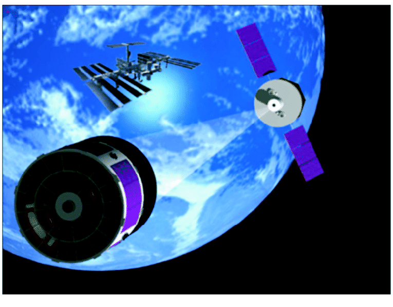
Fig. 1:
ESA-XEUS project: A mirror satellite
reflects X-rays into the detector
satellite, distance 50 m to reach
the spacial resolution
 |
The sensor design goals are:
- very low noise operation (3 electrons equivalent noise
charge);
- best amplification and low power;
- high data rates.
The most interesting results 2004 are:
- a)
- Time integration added;
- b)
- 2D computed doping profiles interpolated to 3D and
- c)
- Qualitative agreement of simulations and experiments for two prototype
designs was reached.
We are in the position to start parameter variations to study the
first amplifier stage in detail by solving the 3D problem on a very
regular basis. The steps considered are:
- Depletion of the sensor volume;
- Removal of the electrons in the internal gate (clear process);
- Collection process of the electrons generated by a single interaction of
one Mn K
 X-ray photon with the silicon crystal;
- Check of the ``read-out'' time (thermal generation creates
electrons, too;
these electrons limit the measurement time and force a new clear process).
Fig. 2:
Detector chamber, the green areas are made up by millions of detector
cells
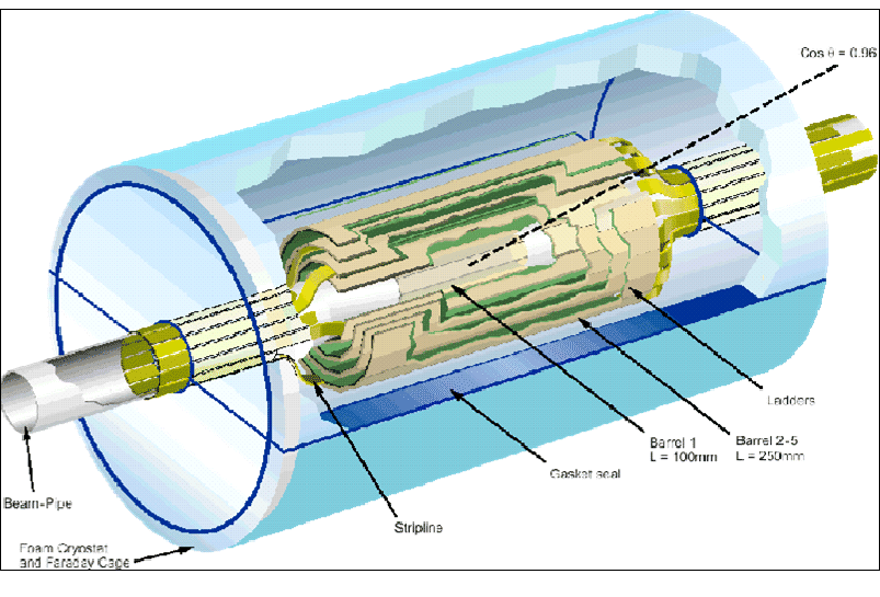 |
Fig. 3:
A computed detection processes (half-cell) is shown in the following
sequence (n(t) - n(0), n(t) electron density):
1600 electrons created 50 ps (upper left), electrons move to the top
300 ps, 400 ps;
horizontal diffusion supported by small fields 1 ns, 3 ns, 10  s
s
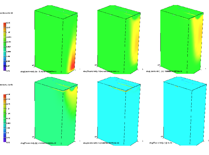 |
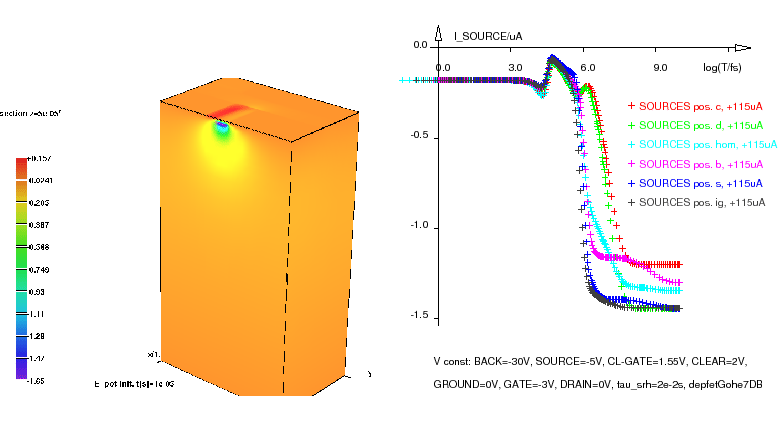
Fig. 4:
Approximately 1296 electrons arrive at the internal gate and cause a
potential (left) and a source contact current difference (right);
contact current signals for different starting positions show the amplification
per electron and the position-dependent losses at the clear contact.
 |
LaTeX typesetting by H. Pletat
2005-07-29